The pursuit of a functional large scale quantum computer has long been hindered by a fundamental conflict between qubit stability and system connectivity. While individual quantum bits can now be controlled with high precision in isolated environments, connecting thousands or millions of them to perform complex error corrected calculations remains a significant engineering hurdle.
Most current architectures suffer from a wiring bottleneck where the physical infrastructure required to manage and link qubits becomes so dense and heat intensive that it destabilizes the very quantum states it intended to support. A recent patent from Nanofiber Quantum Technologies, US12579461B1, proposes a modular solution to this problem by utilizing a hybrid architecture that combines neutral atom qubits with specialized optical fiber links.
The Architecture of Modular Quantum Cells
Traditional monolithic quantum processors attempt to house all necessary components on a single chip. This approach leads to rapid decoherence as the system grows because the proximity of control lines and neighboring qubits introduces unwanted noise. The system described by inventors Hayata Yamasaki and Shinichi Sunami instead adopts a cellular design.
Each quantum computer cell system functions as an independent unit that can be networked with others to form a larger cluster. According to the technical claims, these cells are divided into distinct functional zones including a computing region, a transport region, and an optical link region. This spatial separation allows the system to optimize different physical processes without them interfering with one another.
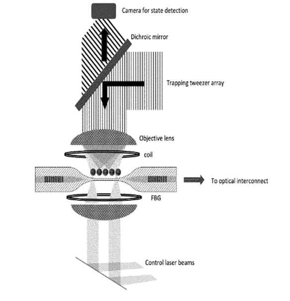
At the heart of each cell is a plurality of qubits, which the patent specifies can include laser coolable atoms, ions, or nitrogen vacancy centers. The system is designed to handle a significant range of qubits, from a single unit up to 100,000 within a modular framework. By using neutral atoms trapped in optical tweezer arrays, the researchers can move information carriers between the different regions of the cell.
This mobility is a critical component of the breakthrough because it allows a qubit to be physically transported from a storage area to a high finesse optical cavity for communication purposes and then back to a computing zone for logic operations.
Bridging Computing and Communication via Nanofibers
The primary technical innovation lies in the optical link module and its integration with the computing region. The patent describes an optical cavity formed by a pair of mirrors with a reflectivity exceeding 90 percent. Specifically, Claim 1 and Claim 4 highlight the use of fiber Bragg grating mirrors that form a cavity coupled to a nanofiber region. In this configuration, atoms are coupled to the evanescent field of the cavity mode near the vicinity of the nanofiber. This setup facilitates a highly efficient interface between the stationary matter qubits and flying photonic qubits.
When an atom is moved into the link region, it can interact with the light trapped in the cavity to generate a photon that is entangled with the atom’s internal state. This photon then travels through an optical interconnect to a separate module. The patent details a photon multiplexer device and a beam splitter measurement unit that facilitate heralded entanglement generation.
By measuring the interference of photons coming from two different cells at a 50 to 50 beam splitter, the system can establish a quantum link between distant qubits. This process, known as an elementary bipartite network, serves as the foundation for the recursive modular architecture.
Recursive Encoding and Error Correction
For quantum computing to be useful, it must overcome the inherent noisiness of quantum hardware. The Nanofiber Quantum Technologies system addresses this through a multi level hierarchy of error correction. Level 1 modules perform local quantum error correction on a small set of physical qubits to create a stable logical qubit. These logical units are then networked to form Level 2 modules where further re encoding takes place to suppress error rates even more.
The engineering details specify that the information processing unit identifies qubit states and decodes error information from syndrome measurement results. Because the cells are connected via optical fibers rather than rigid physical traces, the system can perform gate teleportation. This allows two logical qubits in entirely different physical locations to interact as if they were adjacent. The patent suggests that this method allows for fast suppression of both operation and idle errors, which is a common failure point in static architectures.
Engineering Precision in Transport and Control
The transition of atoms between the free space computing region and the confined optical link requires extreme precision. The system uses objective lenses to focus arrays of optical tweezers that can transport atoms from a first spatial location to a second spatial location. To ensure the qubits remain viable during this move, the patent mentions a storage time ranging from one nanosecond to much longer durations.
Furthermore, the coupling of an individual qubit to the cavity is controlled by its physical position, allowing the electric field coupling to be tuned from zero to a maximum value based on the atom’s proximity to the center of the cavity.
Control is not limited to optical means. The hardware includes a plurality of electrical coil pairs or chip mounted wires designed to control magnetic fields and gradients at the qubit locations. These magnetic fields can shift the resonance frequency of specific qubits, providing a method for spatial addressability and selective single qubit control. When combined with Rydberg blockade mechanisms or cavity mediated photon exchange for two qubit CNOT gates, the system provides a comprehensive toolkit for universal quantum logic within a distributed framework.
Broad Implications for Scalable Quantum Infrastructure
The shift toward a modular fiber based architecture represents a departure from the pursuit of the perfect single chip quantum processor. By treating the quantum computer as a network of interconnected cells, this innovation bypasses the physical scaling limits imposed by cryostat volume and wiring density. The use of standard optical components like circulators, switches, and fiber Bragg gratings suggests a path toward quantum hardware that leverages existing telecommunications manufacturing techniques.
While the patent focuses on the hardware and the immediate network topology, the implications extend to the creation of a quantum internet and large scale hybrid quantum classical computing. The ability to link tens of thousands of qubits across a modular array could finally provide the computational overhead necessary for practical applications in drug discovery, materials science, and complex optimization. By solving the interface problem between matter and light at the nanofiber level, this system provides a viable blueprint for the next generation of quantum engineering.
Looking into the future of quantum networks and distributed computing? Fill out the form to receive focused patent insights on scalable quantum system designs and communication technologies.